|
|
 |
|

 |
|
 |
|

|
⊙
PADS200X 소개
1. PADSLOGIC
2.PADS LAYOUT
3.PADS ROUTER |
 |
⊙ PADS LAYOUT의 TOOLBAR 및MENU
1.TOOLBAR
1.1 Drafting
1.2 Design
1.3 Dimensioning
1.4 ECO
1.5 BGA
2.MENU
2.1 File
2.1.1 New
2.1.2 Open
2.1.3 Save
2.1.4 Save as
2.1.5 Import
*ASC , DXF , ECO Data import
2.1.6 Export
*ASC ,DXF 로의 파일변환
2.1.7 Save As Start-up File
2.1.8 Set Start-up File
2.1.9 Library
*Library List 추가 및 관리요령.
2.1.10 Report
2.1.11 CAM
*Gerber Setting 및 작성 요령.
2.1.12 CAM Plus
2.2 Edit
2.2.1 Copy As Bitmap
2.2.2 Move
2.2.3 Delete
2.2.4 Find
2.2.5 Highlight
2.2.6 Unhighlight
2.2.7 Filter
2.2.8 Properties
2.3 View
2.3.1 Zoom
2.3.2 Board
2.3.3 Extents
2.3.4 Nets
2.3.5 Clearance
2.4 Setup
2.4.1 Pad Stacks
2.4.2 Drill Pairs
2.4.3 Jumpers
2.4.4 Design Rules
*Rules Setting 요령
2.4.5 Layer Definition
*Layer Setting 및 추가, 삭제
요령
2.4.6 Set Origin
2.4.7 Display Colors
2.5 Tools
2.5.1 PCB Decal Editor
*부품 작성 실습
2.5.2 Disperse Components
2.5.3 Length Minimization
2.5.4 Pour Manager
2.5.5 Verify Design
2.5.6 Compare ECO
2.5.7 Macros
2.5.8 Basic Scripts
2.5.9 Options
⊙ PADS LAYOUT 실습
(실습용 데이터 일부 제공 예정)
+AutoCad File Import(기구
데이터)
+Board Outline Drawing
+Orcad Capture에서 Parts
, Netlist Import
+Option 및 Design Rule Setting
+부품배치
+Route
+CAM 작업 |


|

1. Librarian
: Geometry, Mapping File, Catalog,
Catalog Entry Creation
(PCB Property 사용한 Symbol,
Schematic Create and Edit)
2. Package : Schematic Drawing and
Physical Part Packaging
3. Layout : Placement & Route
Automatic,
Semi-Automatic and Interactive Placement
and Routing
4. Fablink : PCB Fabrication Data
Creation
(Gerber, Drill
Data, Drawing Data, Aperture List,
Drill List, Drill Data, etc) |
1st Step
Design Manager
Creating a Schematic
Saving Schematics
Board Geometry
Creating a Board Outline
Saving Board Geometry
|
 |
2nd
Step
Component Geometries
Catalog Files
Invoking PACKAGE
Automatic Packaging
Invoking LAYOUT
Placing Components
Design Rules for LAYOUT
|
 |
3rd
Step
Interactive Routing
Board Station RE
Creating Area Fills
Creating Artwork Data
Creating a Drill Table
Creating Fabrication Drawings |
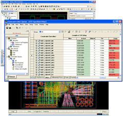 |

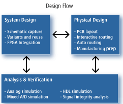
Cadence® Allegro® PCB Design offers the leading physical and electrical
constraint-driven PCB layout and interconnect routing system.
The fully integrated design flow includes design creation, library
creation, placement, interactive routing and editing, automatic routing,
and interfaces for manufacturing and mechanical CAD.
The user interface is intuitive, easy-to-use, and consistent throughout the
design flow.
Large, dense PCB designs with high-speed interfaces can utilize Global
Routing Environment technology
for intelligent interconnect planning and routing automation.
Features/Benefits
- Provides a scalable, full-featured PCB design solution
- Enables a constraint-driven design flow to reduce design iterations
- Provides a single, consistent, front-to-back constraint management
environment
- Delivers an integrated RF/analog design and mixed-signal design
environment
- Provides interactive floorplanning and component placement
- Provides design partitioning for large, dispersed development teams
- Enables real-time, interactive push/shove etch editing
- Allows real-time plowing/healing with dynamic shape technology
- Manages net scheduling, timing, crosstalk, layer set routing, and
geometric constraints
- Provides proven PCB Router technology for auto-routing of random signals
- Captures design intent for interconnects through hierarchical flow
planning
- Shortens interconnect planning and routing time for dense designs with
high-speed interfaces
- Outputs design data in a variety of manufacturing formats
|
|
|
|
 |
|
 |
|
|
|